FABRICATION
ELECTRON-BEAM/FIB LITHOGRAPHY
FOCUS OF RESEARCH
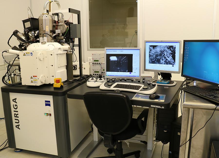
The Electron Beam Lithography system at the CRNN is a versatile instrument, incorporating a cross-beam system (Zeiss Auriga) with a FESEM column and a FIB column. Both the electron and ion beams can be controlled using a RAITH system, which also controlls a piezo stage for accurate control of the substrate position. The electron beam writing has a resolution of ~10nm.
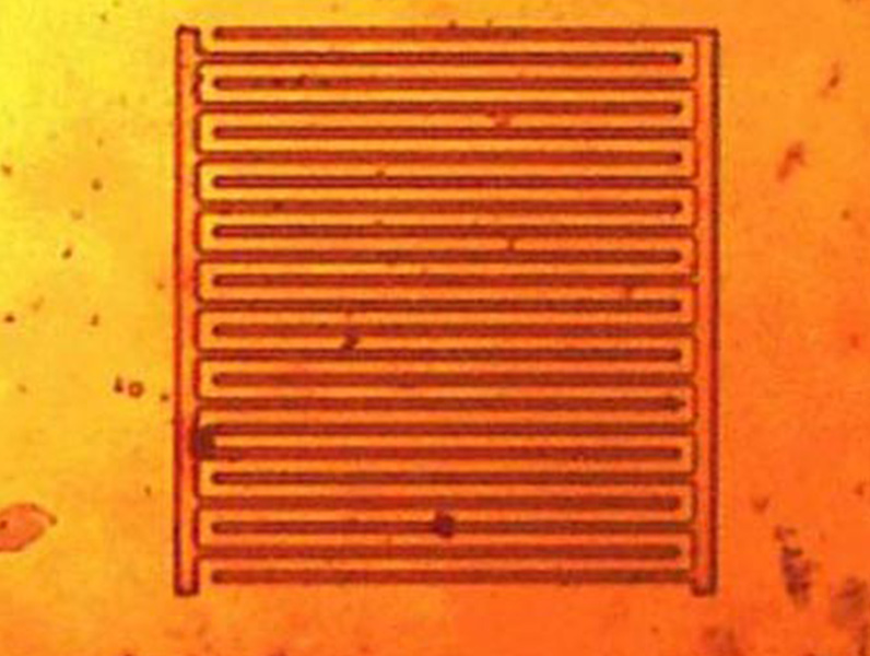
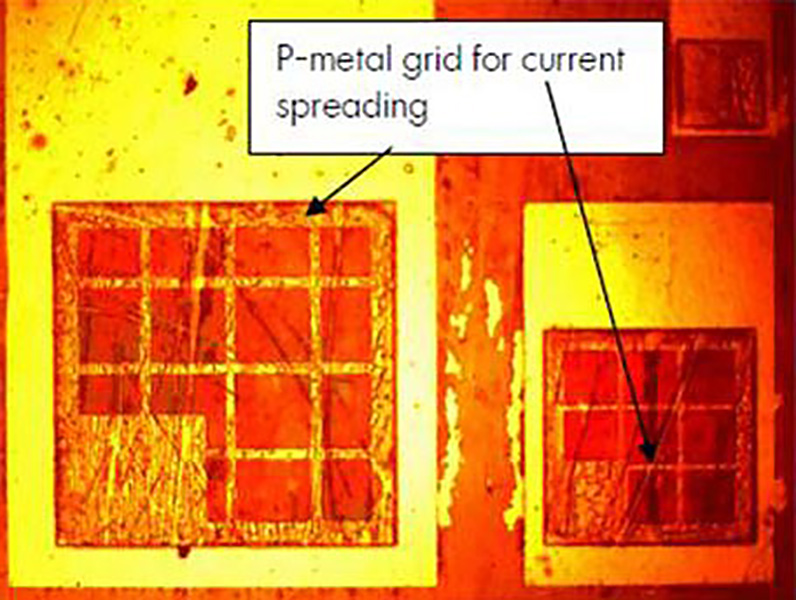
A number of gas sources are also incorporated in the system, which in conjunction of the ion beam is capable of "writing" patterns of various metals with nanometer scale resolutions. The same technique can also be used for nanoscale etching of silion and silicon dioxide.
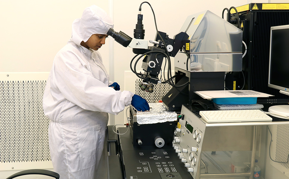
An in-situ probing system has also been installed for allowing direct electrical measurements on the as-fabricated device without breaking vacuum.
EQUIPMENT DETAILS
| TITLE | DESCRIPTION |
| Model | Zeiss Auriga |
| Resolution | 1nm for FESEM imaging |
| 13nm for e-beam lithography | |
| FIB | CANION 31 |
| Resolution | 7 nm |
| GIS | Deposition of Au, Pt SiO2 |
| Etching of SiO2 and C | |
| Stage | Kleindiek |
| Resolution 0.5nm | |
| Probes | Micromanipulator MM3A |
| 3 probe sets | |
| Z resolution 0.5nm | |
| XY resolution 2.5nm |
EZEISS AURIGA with RAITH ELPHY PLUS and KLEINDIEK Stage and Probes
MASK ALIGNER FOR OPTICAL LITHOGRAPHY
SUSS MA/BA 6
The SUSS MicroTec mask aligner and bond aligner system at the CRNN has been configured for wafer sizes ranging from small pieces to 6-inch in diameter. Masks up to 7 inch x 7 inch can be used in the system.
The resolution for top side alignement is 0.5nm. Back side alignement facilities using two video microscopes is also incorporated.
SUSS MA/BA 6
SUSS MA/BA 6